Zone melting
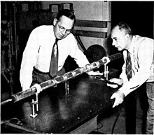
(right) Vertical zone refining, 1961. The induction heating coil melts a section of the metal bar in the tube. The coil moves slowly down the tube, moving the molten zone to the end of the bar.
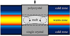
Zone melting (or zone refining, or floating-zone method, or floating-zone technique) is a group of similar methods of purifying crystals, in which a narrow region of a crystal is melted, and this molten zone is moved along the crystal. The molten region melts impure solid at its forward edge and leaves a wake of purer material solidified behind it as it moves through the ingot. The impurities concentrate in the melt, and are moved to one end of the ingot. Zone refining was invented by John Desmond Bernal[1] and further developed by William G. Pfann[2] in Bell Labs as a method to prepare high-purity materials, mainly semiconductors, for manufacturing transistors. Its first commercial use was in germanium, refined to one atom of impurity per ten billion,[3] but the process can be extended to virtually any solute–solvent system having an appreciable concentration difference between solid and liquid phases at equilibrium.[4] This process is also known as the float zone process, particularly in semiconductor materials processing.


Process details
[edit]The principle is that the segregation coefficient k (the ratio at equilibrium of an impurity in the solid phase to that in the liquid phase) is usually less than one. Therefore, at the solid/liquid boundary, the impurity atoms will diffuse to the liquid region. Thus, by passing a crystal boule through a thin section of furnace very slowly, such that only a small region of the boule is molten at any time, the impurities will be segregated at the end of the crystal. Because of the lack of impurities in the leftover regions which solidify, the boule can grow as a perfect single crystal if a seed crystal is placed at the base to initiate a chosen direction of crystal growth. When high purity is required, such as in semiconductor industry, the impure end of the boule is cut off, and the refining is repeated.[citation needed]
In zone refining, solutes are segregated at one end of the ingot in order to purify the remainder, or to concentrate the impurities. In zone leveling, the objective is to distribute solute evenly throughout the purified material, which may be sought in the form of a single crystal. For example, in the preparation of a transistor or diode semiconductor, an ingot of germanium is first purified by zone refining. Then a small amount of antimony is placed in the molten zone, which is passed through the pure germanium. With the proper choice of rate of heating and other variables, the antimony can be spread evenly through the germanium. This technique is also used for the preparation of silicon for use in integrated circuits ("chips").[citation needed]
Heaters
[edit]A variety of heaters can be used for zone melting, with their most important characteristic being the ability to form short molten zones that move slowly and uniformly through the ingot. Induction coils, ring-wound resistance heaters, or gas flames are common methods. Another method is to pass an electric current directly through the ingot while it is in a magnetic field, with the resulting magnetomotive force carefully set to be just equal to the weight in order to hold the liquid suspended. Optical heaters using high-powered halogen or xenon lamps are used extensively in research facilities particularly for the production of insulators, but their use in industry is limited by the relatively low power of the lamps, which limits the size of crystals produced by this method. Zone melting can be done as a batch process, or it can be done continuously, with fresh impure material being continually added at one end and purer material being removed from the other, with impure zone melt being removed at whatever rate is dictated by the impurity of the feed stock.[citation needed]
Indirect-heating floating zone methods use an induction-heated tungsten ring to heat the ingot radiatively, and are useful when the ingot is of a high-resistivity semiconductor on which classical induction heating is ineffective.[citation needed]
Mathematical expression of impurity concentration
[edit]When the liquid zone moves by a distance , the number of impurities in the liquid change. Impurities are incorporated in the melting liquid and freezing solid.[5][clarification needed]
- : segregation coefficient
- : zone length
- : initial uniform impurity concentration of the solidified rod
- : concentration of impurities in the liquid melt per length
- : number of impurities in the liquid
- : number of impurities in zone when first formed at bottom
- : concentration of impurities in the solid rod
The number of impurities in the liquid changes in accordance with the expression below during the movement of the molten zone
Applications
[edit]Solar cells
[edit]In solar cells, float zone processing is particularly useful because the single-crystal silicon grown has desirable properties. The bulk charge carrier lifetime in float-zone silicon is the highest among various manufacturing processes. Float-zone carrier lifetimes are around 1000 microseconds compared to 20–200 microseconds with Czochralski method, and 1–30 microseconds with cast polycrystalline silicon. A longer bulk lifetime increases the efficiency of solar cells significantly.[citation needed]
High-resistivity devices
[edit]It's used for production of float-zone silicon-based high-power semiconductor devices.[6]: 364
Related processes
[edit]Zone remelting
[edit]Another related process is zone remelting, in which two solutes are distributed through a pure metal. This is important in the manufacture of semiconductors, where two solutes of opposite conductivity type are used. For example, in germanium, pentavalent elements of group V such as antimony and arsenic produce negative (n-type) conduction and the trivalent elements of group III such as aluminium and boron produce positive (p-type) conduction. By melting a portion of such an ingot and slowly refreezing it, solutes in the molten region become distributed to form the desired n-p and p-n junctions.[citation needed]
See also
[edit]- Fractional freezing a.k.a. freeze distillation
- Monocrystalline silicon
- Wafer (electronics)
Further reading
[edit]- Hermann Schildknecht (1966), Zone Melting, Weinheim: Verlag Chemie
- Müller, G. (1988). Crystal Growth from the Melt. Crystals. Vol. 12. Berlin, Heidelberg: Springer Berlin Heidelberg. ISBN 978-3-642-73210-2. Retrieved 2023-11-23.
References
[edit]- ^ Brown, Andrew (2005-11-24). J. D. Bernal: The Sage of Science. OUP Oxford. ISBN 9780198515449.
- ^ William G. Pfann (1966) Zone Melting, 2nd edition, John Wiley & Sons
- ^ ”Zone melting”, entry in The World Book Encyclopedia, Volume 21, W-X-Y-Z, 1973, page 501.
- ^ Float Zone Crystal Growth
- ^ James D. Plummer, Michael D. Deal, and Peter B. Griffin (2000) Silicon VLSI Technology, Prentice Hall, page 129
- ^ Sze, S. M. (2012). Semiconductor devices: physics and technology. M. K. Lee (3 ed.). New York, NY: Wiley. ISBN 978-0-470-53794-7. OCLC 869833419.


